Clock Domains
The Core-v-mcu has three major clock domains that are all derived from the input reference clock.
SoC clock is used to drives the CV32E40P cpu and memory subsystem.
Periph clock is used for the UDMA peripherals to generate the various clocks required for the peripherals
FPGA clock is used as the primary clock to the eFPGA.
The Input reference clock is assumed to be 10 MHz. It feeds a Verisilicon PLL which creates the primary high speed clock. The High speed clock drives three independent divisors that are used to generate the the three domains. Additionally, an additional divisor is provided to reduce the frequency of the reference clock to the various timer resources.
The following is a Block diagram of the Clock Domains
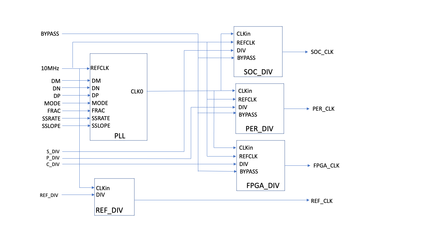
PLL Description
The Verisilicon PLL has the following Input control signals that are sourced from the APB_PLL register Block.
DM[5:0] Reference Input Divider Control Pins. Sets the reference divider factor from 1 to 63.
DN[10:0] Feedback Divider Control Pins. Sets the feedback divider factor from 16 to 2047.
DP[2:0] Output Divider Control Pins. Sets the post divider factor from 1 to 7.
PD PLL Power Down Signal. 1: PLL power down, 0: normal operation
PDDP Post Divider Power Down Signal. 1: DP power down, 0:DP normal operation
RESETN Resets the SSC & Fraction Function when low
MODE[1:0] 00: integer mode, 01: fraction mode, 10: spread spectrum mode, 11: reserved.
SSRATE[10:0] Spreading Frequency Control. Set the triangle modulation frequency.
SLOPE[23:0] Spreading Slope Control. Set the spread step
FRAC[23:0] Fractional Portion of DN Value.
BYPASS PLL BYPASS 0: Normal operation, 1: PLL bypass
Clock Divisors
The output of the PLL is divided by 10-bit divisors to create the SoC clock, the peripherial Clock and the Primary FPGA clock. An Additional divisor reduces the input reference clock.